Timers#
Many of the sequential logic circuits we’ve discussed require the input of a regular square wave to act as a clock and synchronize the timing of all the different components. In this section, we’ll explore a few different ways of generating this square wave.
Schmitt Inverter Wave Generator#
Recall an RC circuit when charging:
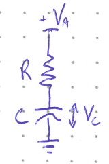
The charge at the top of the capacitor is: \(V_c(t) = V_A \left(1 - e^{-t/RC}\right)\), and the max potential is \(V_A\).
When discharging:
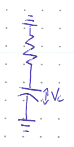
Here, \(V_c(t) = V_0 \, e^{-t/RC}\) where \(V_0\) is the initial charge that had built up on the capacitor.
We can make a clock generator by attaching a Schmitt Inverter to an RC circuit.
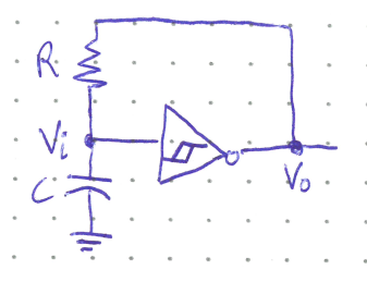
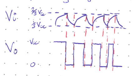
Let’s use as an example the case where the Schmitt Trigger levels are \(\frac{1}{3}V_{cc}\) and \(\frac{2}{3}V_{cc}\) and see how this generates a regular square wave.
Suppose initially \(V_i\) is low. This makes \(V_o\) high, and starts to charge the capacitor, slowly increasing \(V_i\). Once \(V_i\) rises above \(\frac{2}{3}V_{cc}\), \(V_o\) will switch to low (0 V), and the capacitor will start discharging, thus lowering \(V_i\) again. Once it goes below \(\frac{1}{3}V_{cc}\), the inverter output will switch to high again and the cycle will repeat. This process is shown in the timing diagram below.
Now let’s determine how long the the wave spends in each of the high and low states.
How long is the capacitor charging for? I.e. how long is the output in the high state?
The charging formula assumes that the initial voltage on the capacitor is 0 V. Thus to find the time it takes to go from \(\frac{1}{3}V_{cc}\) to \(\frac{2}{3}V_{cc}\), we have to find the time to go from \(0 \to \frac{1}{3}V_{cc}\) and subtract it from the time to go from \(0 \to \frac{2}{3}V_{cc}\). Let’s define \(t_2\) as the time to charge from 0 V all the way to the upper threshold, and \(t_1\) the time it takes to go from 0V to the lower threshold. Then, \(t_{charging} = t_{2} - t_{1}\).
First let’s calculate \(t_{2}\):
Similarly, for \(t_{1}\):
and thus:
By changing the resistance and capacitance we can control the charging time!
For discharging, we have the much easier task of determining how long it takes for the capacitor to discharge from the high threshold to the low threshold. How long is the capacitor discharging, i.e. how long does the wave generator’s output in the low state?
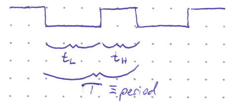
In this setup, the discharge time is exactly equal to the charging time! This is not true in general, but arises from our choice of threshold levels. In general, we define a quantity called the duty cycle (\(D\)) of a square wave: that is the percentage of time spent in the high state.
The 555 Timer#
Finally, we come to the 555 timer, a common IC used to generate a clock signal. The name comes from three 5 kΩ resistors that are used to set threshold voltages of comparators.
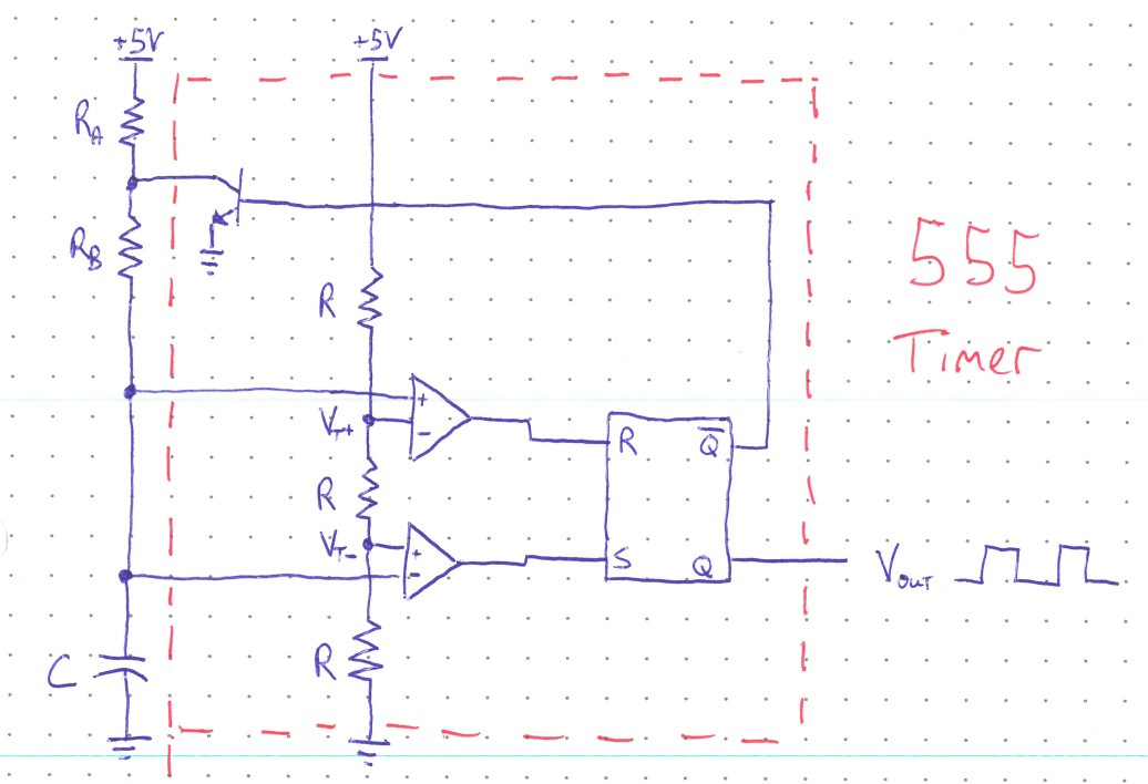
When the output voltage \(Q\) of the SR Latch is high, \(\bar{Q}\) is low, and the control transistor is thus in cutoff mode meaning no current can flow from collector to emitter. This leads to the capacitor charging.
Once the voltage between \(R_B\) and \(C\) rises above \(V_{T+}\) (\(= \frac{2}{3}V_{cc}\)), this triggers the reset on the latch. \(Q\) switches to low and \(\bar{Q}\) to high. This allows current to flow through the transistor, and the capacitor discharges until the voltage between \(R_B\) and \(C\) falls below \(V_{T-}\) (\(= \frac{1}{3}V_{cc}\)). This sets \(Q\) to high again and the cycle starts anew.
Note that the capacitor charges through \(R_A\) & \(R_B\), but discharges solely through \(R_B\). Thus:
Aside: Crystal Oscillators
Instead of using RC circuits, most computers use quartz crystal oscillators as a clock, which are far more precise. The quartz crystal is deformed by an electric field. If the field is removed, the crystal snaps back to its original shape. But the movement of the crystal creates another electric field. If this is fed back to the crystal it will oscillate at a resonant frequency determined by the shape and size of the crystal.