CMOS Logic Family#
The TTL family uses bipolar junction transistors (BJTs), which we have discussed extensively previously. A second commonly used Logic Family is the CMOS logic family, where CMOS stands for Complimentary Metal Oxide Semiconductor. This logic family uses a different type of transistor called a MOSFET (Metal Oxide Semiconductor Field Effect Transistor) and is highly prevalent in electronics, particularly processors and memory chips.
A MOSFET transistor works using similar principles to a BJT, but instead of current applied through the base determining whether the transistor is ON or OFF, MOSFETs are voltage driven. This has several advantages, namely because there is no current, there is less power dissipation. As well there is no need for resistors to dissipate power, and thus MOSFETs can be made smaller and generate less heat. On the other hand, MOSFETs are extremely sensitive to static electricity, and are slightly slower than TTL chips. These advantages and disadvantages are summarized below:
TTL
Advantages:
fast switching
more durable
great for hobbyists or education, or for labs where custom circuits need to be built and taken apart often
Disadvantages:
Consume a lot of power (lowest power is \(\sim 1\,\text{mW}\))
Many components mean large profile (cannot be tightly packed)
Generate a lot of heat
more expensive to make
CMOS
Advantages:
low power (typically \(1\,\text{nW}\))
low heat
can be tightly packed
cheap to produce
high Fan Outs (\(\sim 50\))
Disadvantages:
sensitive to static
slightly slower switching times
MOSFET Interior#
Now we will look at how a MOSFET is constructed, and how they are used in CMOS logic gates to achieve the above advantages. There are two types of MOSFETs, enhancement and depletion, but we will focus on enhancement MOSFETs, which are the more common type.
Just as BJTs can be constructed of NPN or PNP semiconductor sandwiches, MOSFETs can be either P-channel or N-channel type.
N-Channel#
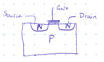
Notice the similarity to the NPN sandwich structure of a BJT. However, here the two negatively doped components are attached to terminals labelled “Source” and “Drain”. Between this is a “Gate” separated from the semiconductors by an insulator (traditionally a thin layer of metal oxide, hence the name MOS).
When a positive voltage relative to the middle P-region is applied at the gate, it pushes away the positive charged holes in the middle P region, and attracts electrons from the N-doped regions. As long as the gate voltage is greater than some threshold (typically \(+1.5\,\text{V}\)), there will be enough \(e^-\) attracted near the gate to create a thin, N-doped channel connecting the source and drain.
Without the connecting channel, the depletion regions at the NP junctions make it so the effective resistance between source and drain is extremely high, \(\sim 10^{10}\,\Omega\). With the channel, however, the resistance of the MOSFET is much lower, approximately only \(1\,\text{k}\Omega\). So, by applying voltage at the gate, we can effectively toggle the resistance of the MOSFET from \(\sim \infty\) to \(\sim 1\,\text{k}\Omega\). This is where the name “Field Effect Transistor” comes from. By applying a voltage (aka electric field) at the gate, we can turn the transistor ON or OFF like a switch.
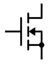
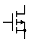
The schematic symbol for an N-channel mosfet is shown below. The left-most terminal is the Gate, the upper one the Drain, and the lower one the Source. The three broken dashes are meant to represent that this is an enhancement MOSFET (the channel is not present by default), and the arrow pointing inward signifies that it is an N-channel (Although I don’t think this is the true intent, I use the arrow to remember which terminal needs to have high voltage applied to turn the MOSFET on; in this case, the Gate must be positive). The terminal connected to two of the dashes (the lower one in this image) is always the Source, which is internally connected to the middle substrate. To see if the Gate voltage is High or Low, it is always compared to the Source voltage.
P-Channel#
A P-channel MOSFET works similarly, just with the doping reversed, and is activated by a negative voltage at the Gate relative to the Source.
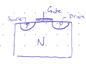
The schematic symbol for a P-channel MOSFET has the arrow pointing outward (again I use this to remember that higher voltage should be applied at the Source to turn the transistor ON)
Summary#
Here is a table summarizing how to connect P-Channel and N-Channel MOSFETs, and their behaviour:
Type |
Drain Connected to |
Source Connected to |
\(V_{GS}\) needed to activate |
\(R_{ON}\) |
\(R_{OFF}\) |
|---|---|---|---|---|---|
P-Channel |
Low |
High |
\(-1.5\,\text{V}\) (i.e. Gate Low) |
\(1\,\text{k}\Omega\) |
\(10^{10}\,\Omega\) |
N-Channel |
High |
Low |
\(+1.5\,\text{V}\) (i.e. Gate High) |
\(1\,\text{k}\Omega\) |
\(10^{10}\,\Omega\) |
Aside: Depletion MOSFETS
A depletion MOSFET works by having the channel present by default, and then driven away by an applied voltage. Its symbol is very similar, but contains a solid line where an enhancement MOSFET symbol is dashed.
Complimentary MOSFET Logic Gates#
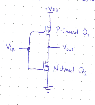
To make logic gates with MOSFETs, one of each type (N-channel and P-channel) are used in a complimentary fashion as a voltage divider. For example, here is a CMOS inverter:
\(V_{in}\) |
\(Q_1\) |
\(Q_2\) |
\(V_{out}\) |
|---|---|---|---|
High |
OFF |
ON |
\(0\,\text{V}\) |
Low |
ON |
OFF |
\(\sim V_{DD}\) |
Note that because of the near infinite resistance when one of the MOSFETs is OFF, no current flows from \(V_{DD}\) to ground.
Finally, here is an example of a CMOS NAND gate. Compare its simplicity with the equivalent TTL gate.
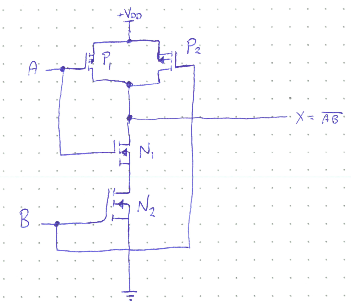
When both A & B are high, \(N_1\) and \(N_2\) are ON, but \(P_1\) and \(P_2\) are off, meaning their resistance is approximately infinite. This effectively connects the output X to ground. Conversely, when either A or B (or both) are low, one of the P transistors will be ON, and one of the N transistors OFF. This effectively connects X to \(V_{DD}\) and disconnects it from ground.
Similarly to TTL, there are different subfamilies of CMOS:
Subfamily |
Description |
Prop. Delay (ns) |
|---|---|---|
74HC |
“High Speed CMOS” (in quotes because newer subfamilies are faster) |
8 |
74AC |
Advanced CMOS |
4.7 |
74AHC |
Advanced High Speed CMOS |
4.3 |