Adders#
Adder circuits are circuits that perform binary addition, and in many cases subtraction as well using the 2’s complement system. The entire addition operation is typically carried out by a large assembly called the Arithmetic Logic Unit (ALU), but at its core are circuits that simply perform the bit-by-bit addition in each column as a logic operation.
Adder logic circuits for one bit come in two types:
Half Adder: Has two inputs (\(A\) & \(B\)) and two outputs: the Sum (\(S\)) and Carry (\(C_{out}\)).
Full Adder: Can also take an additional input \(C_{IN}\), the carry bit from another adder. A Full Adder can be constructed from two half adders.
Full Adder Logic#
What does the inner circuitry of a Full Adder look like? Let’s use a K Map to design one. First we will make a truth table, recalling how addition works.
\(A\) |
\(B\) |
\(C_{in}\) |
\(C_{out}\) |
\(S\) |
|---|---|---|---|---|
0 |
0 |
0 |
0 |
0 |
0 |
0 |
1 |
0 |
1 |
0 |
1 |
0 |
0 |
1 |
0 |
1 |
1 |
1 |
0 |
1 |
0 |
0 |
0 |
1 |
1 |
0 |
1 |
1 |
0 |
1 |
1 |
0 |
1 |
0 |
1 |
1 |
1 |
1 |
1 |
For \(S\) The K-map looks like so:
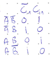
There are not really any simplifying loops we can do, but remember that the checkerboard pattern means the circuit diagram can be be made more compact with XOR gates.
For \(C_{out}\):
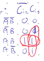
Here, we do have some loops and the sum-of-products expression is simply
The final full adder circuit is shown below. This circuit will add, at most, three one-bit numbers.
[Figure: Logic circuit implementation. Inputs A, B, and C run down the left side. Two cascaded XOR gates produce \(S\) (A XOR B, then XOR C). Three AND gates (for AB, BC, and AC) feed into an OR gate producing \(C_{out}\).]
Parallel Adder#
Since we usually want to sum binary numbers with more than one bit, several adders are chained together to create a Parallel Adder. Here is an example of a 4-bit Parallel Adder.
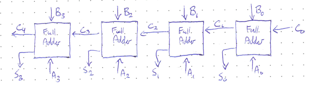
The right-most adder is the Least Significant Bit, and could be implemented with a half-adder since there would be no carry input. However, we shall soon see that it is still useful to have a Full Adder in the LSB place.
An important consideration is carry-bit propagation. Each full adder cannot give the correct answer until it receives the correct carry-in from the previous adder. That means that in this set up, the time it takes to add N-bit numbers scales linearly with the number of bits. If each full adder has a propagation delay of \(t_P\), then it takes \(Nt_P\) seconds to arrive at the correct answer. If speed is an important consideration, calculation time can be improved by having a separate circuit dedicated to calculating each carry-bit individually directly from the numbers being added. This is known as a Carry Look Ahead adder, and it is significantly faster than the parallel adder above, but comes at the cost of significantly increasing circuit size, complexity, and power consumption.
ALU#
To control timing considerations and determine which numbers are being added processors have an Arithmetic Logic Unit (ALU). The ALU will have a parallel adder at its center (possibly with Carry Look Ahead functionality) as well as two registers called the A register (also known as the Accumulator) and the B register, and a control unit. The control unit coordinates loading values from memory addresses, clearing the registers, and sending signals to perform the summation operation.
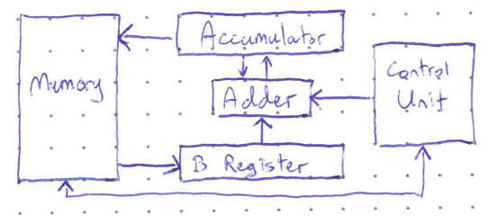
Let’s walk through the steps to add two numbers 1001 and 0101 together. ALLCAPS terms are signals sent from the control unit.
CLEAR to make [A] 0000.
LOAD first number (say 1001) into the [B]. The sum from the adders is now 1001 as well, but note that it hasn’t been moved to Accumulator yet.
TRANSFER to move the sum output of the parallel adder to [A], now 1001.
LOAD to put next number (0101) into [B]. Sum becomes 1110.
TRANSFER to set [A] to the desired sum. This overwrites what was in [A] and replaces it with the entire sum of 1110.
If finished, [A] can be output to memory. If you want to add another number, go back to step 4 and transfer a new value into [B]. Repeating steps 4 and 5 will continue to add to the accumulator (hence the name).
Below is a more complete look at how the registers and parallel adder are connected together.
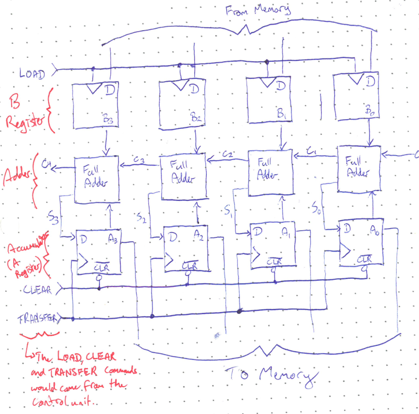
So why keep \(C_0\) as an input? It is so that we can use this same parallel adder to subtract as well as add.
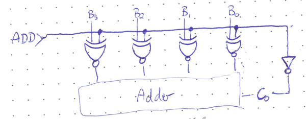
Let’s put in another flag from the control unit. An ADD command that is level triggered, so that ADD = 1 will add A+B, and ADD = 0 will lead to subtraction of A−B. When ADD is 0, we want to turn B into its 2’s complement. Recall that a number’s 2’s complement was found by flipping the bits and adding 1. This is why \(C_0\) is useful, it can be used to perform the “add 1”.
Place the following logic component in between the B register and the adder, and your adder can now subtract as well:
I guess when performing subtraction through addition more is less?