TTL#
TTL, or Transistor-Transistor Logic, has been an available standard for approximately 50 years, and is still the standard for hobbyists and educational purposes, but has been superceded in professional applications. Below is an example of a TTL NAND gate:
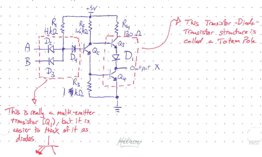
Let’s go through the workings of the above circuit to confirm that it is indeed a NAND operation.
Consider the case where both A & B are high:
Diodes \(D_2\) and \(D_3\) are thus reverse biased, and no current flows through them.
We now will look at each of the transistors (\(Q_2\), \(Q_3\), and \(Q_4\)) to determine if they are in cut-off mode (OFF) or if they allow current to flow from collector to emitter (ON).
Note in particular, that \(Q_4\) cannot be ON unless \(Q_2\) is also on.
Since \(D_2\) and \(D_3\) are reversed biased, current will definitely flow down through \(R_1\) and across \(D_4\) and the BE junction of \(Q_2\), turning it ON.
This implies that \(Q_4\) is also ON.
Since \(Q_4\) is conducting current and in saturation, the potential drop across the CE junction is \(\sim 0\,\text{V}\).
Therefore the output voltage at X is also very small and the output signal is low.
What about \(Q_3\)? Is it ON or OFF?
Since \(V_{B\text{-}Q_4} \sim 0.72\) and \(Q_2\) is ON and in saturation, the voltage at the base of \(Q_3\) is also \(\sim 0.72\,\text{V}\). This would normally be enough to turn \(Q_3\) on if it were by itself, but the diode \(D_1\) adds another \(0.7\,\text{V}\) to the potential barrier, effectively doubling it.
\(Q_3\) is thus OFF and no current flows through \(R_4\) when X is low. This is important because whenever current flows through a resistor there is power dissipation. To save power, the Totem Pole arrangement is used to stop current flow whenever X is low.
Now consider the case when either A or B (or both) are connected to ground and thus low:
\(D_2\) or \(D_3\) are now forward biased and current will flow from the supply through the input.
This makes the voltage between \(D_2\) & \(D_4\) only \(0.7\,\text{V}\), which is not enough to overcome the barrier of \(D_4\) + \(Q_2\)’s BE junction.
\(Q_2\) is thus OFF.
Because \(Q_2\) is not conducting, neither can \(Q_4\).
\(Q_3\), however, is ON, allowing current to flow out of X and making it a high signal.
Summary Table:
A |
B |
\(Q_2\) |
\(Q_3\) |
\(Q_4\) |
X |
|---|---|---|---|---|---|
0 |
0 |
OFF |
ON |
OFF |
1 |
0 |
1 |
OFF |
ON |
OFF |
1 |
1 |
0 |
OFF |
ON |
OFF |
1 |
1 |
1 |
ON |
OFF |
ON |
0 |
NAND confirmed!
To restate something that may have been missed: The purpose of the totem pole structure is to ensure that \(Q_3\) and \(Q_4\) are never both conducting at the same time. This saves power by making sure current can’t flow straight to ground from the source.
Additionally, the two inputs are connected to high through resistors if there is no input at all (i.e. if pins are left floating). This is why floating pins are high for TTL chips.
Now, consider that when X is low, current flows in to X and through \(Q_4\) to ground if the gate is connected to something. Similarly, when the output is connected to something, current flows out through \(Q_3\) and X. The more “load” on X (i.e. the more things connected), the higher the current.
Recall that transistors are only saturated when their BE current is a substantial fraction of the CE current, and if the CE current increases to \(\sim 100\) times the BE current, then the transistor is in amplification mode rather than saturation. Also recall that in amplification mode, \(V_{CE} > 0.7\) and can get quite high.
Our derivations above confirming proper NAND gate operation relied on saturation and \(V_{CE}\) of \(Q_4\) and \(Q_3\) being \(\sim 0\) when conducting. Therefore, if too much load, and hence too much current, is present, the output values at X will cease to be correct because of the lack of saturation. So for example, X could output High even if A & B are both high because of the non-zero potential across \(Q_4\)’s CE junction.
This limit to the load on X is usually expressed as “Fan Out”, defined as the maximum number of similar gates that can be driven by the output.
There are different flavours of TTL family called series, or sometimes subfamilies. The different subfamilies provide a range of speeds, power consumptions, and costs. They are labelled by the numbers and letters in the name of the IC.
74 – Standard TTL
74S – Schottky TTL – faster switching capabilities
74LS – Low Power Schottky
74AS – Advanced Schottky – even faster switching
74ALS – Advanced Low Power Schottky
74F – Fast TTL – newer and faster
Comparison:
74 |
S |
LS |
AS |
ALS |
F |
|
|---|---|---|---|---|---|---|
Prop. Delay (ns) |
9 |
3 |
9.5 |
1.7 |
4 |
3 |
Power Dissipation (mW) |
10 |
20 |
2 |
8 |
1.2 |
6 |
Fan Out |
10 |
20 |
20 |
40 |
20 |
33 |