SR Flip Flop#
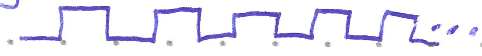
It is often the case that we want circuit components to only be able to change state at fixed times. Typically this is so multiple components can work synchronously. To accomplish this, a clcok signal is used, which is generally a pulse train of square waves.
The clock signal is distributed throughout the circuit to components that can only change state when the clock makes a transition. Such components are thus edge triggered. This is the difference between a latch and a flip flop. Latches are level triggered, whereas flip flops are edge triggered.
The triggering edge can either be a positive going transition (\(\uparrow\), clock changes from low to high), or a negative going transition (\(\downarrow\), clock changes from high to low). A common convention is to label the triggering input with a triangle, and if the triggering transition is negative going put a not bubble in front of the triangle (do not confuse with a NOT gate).
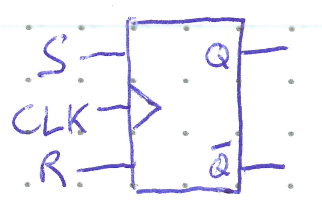
There are several types of flip flops, but we will begin with the SR flip flop pictured above, whose behaviour is described by the following pseudo truth table.
\(S\) |
\(R\) |
\(CLK\) |
Output |
|---|---|---|---|
0 |
0 |
\(\uparrow\) |
No Change |
0 |
1 |
\(\uparrow\) |
\(Q = 0\) |
1 |
0 |
\(\uparrow\) |
\(Q = 1\) |
1 |
1 |
\(\uparrow\) |
Invalid |
Once again, there is an invalid state when both Set and Reset inputs are active on a clock transition. The output will be unpredictable based on small manufacturing variances.
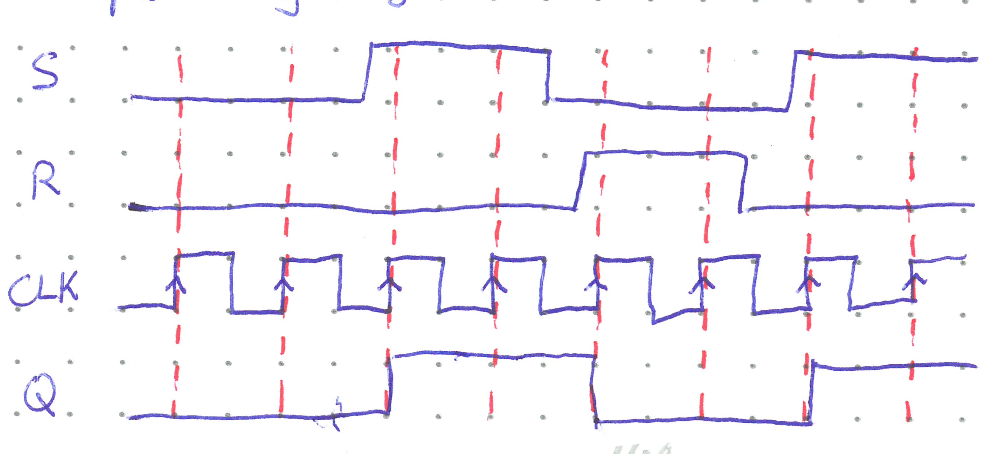
Here is an example timing diagram showing the SR flip flop behaviour. Notice that the output only changes on active clock transitions. These are the only times the \(S\) and \(R\) inputs are checked.
Circuitry#
An SR flipflop consists of the familiar NAND latch, as well as a pulse steering circuit and an edge detector for the clock.
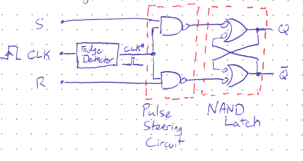
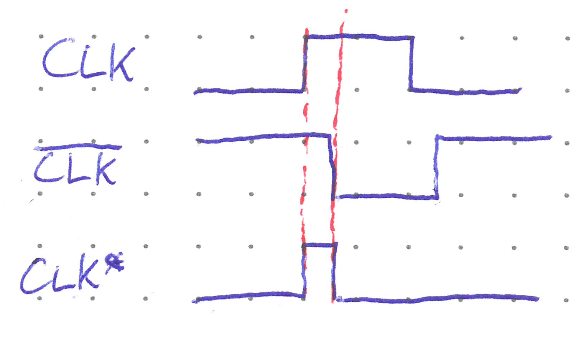
The edge detector turns the clock signal into one that is only high for a very brief instant on a transition, called \(CLK^*\). One way of doing this is described below, but the important thing is the signal going into the pulse steering circuit is only high momentarily. The NAND gates of the pulse steering circuit pass on the appropriate Set and Rest inputs into the latch only when the CLK has a positive going transition. That is, only when \(CLK^* = 1\) can the output of the pulse steering NANDs be anything other than 1. Recall that the NAND latch is active low, and so does nothing if its inputs are both high. The addition of the edge detctor and pulse steering circuit thus turn the latch from being level triggered to being edge triggered, making a flip flop.
There are a few ways of making an edge detector, but an ingenious manner takes advantage of the tiny delay caused by a signal propagating through a logic gate—something that usually only causes trouble.
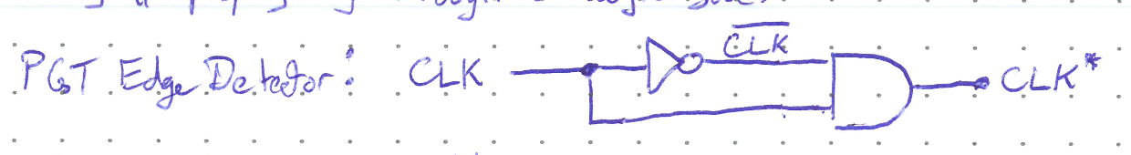
The CLK signal is split into two different path and a NOT gate placed along the top path. Because there will be a small delay before the inversion is complete, the two paths end up out of sync by a few nanoseconds. By ANDing the two signals together, the portion just after the positive going transition is the only part that remains high. If it were not for the delay, one would have expected the AND output to always be low because \(x\bar{x} = 0\) in Boolean algebra. This is an example where it is important to remember that mathematical models are not perfect represenations of reality. Note that the timing diagram pictured is not entirely accurate, because the AND gate should also have a slight delay!